Chungnam National University Team Pioneers Defect-Free High-Quality Graphene Electrodes
PR Newswire
DAEJON, South Korea, Jan. 26, 2026
One-step, etch- free patterning enables clean, low-resistance graphene electrodes for transparent and flexible devices
DAEJON, South Korea, Jan. 26, 2026 /PRNewswire/ -- Transparent electrodes transmit light while conducting electricity and are increasingly important in bioelectronic and optoelectronic devices. Their combination of high optical transparency, low electrical resistance, and mechanical flexibility makes them well suited for applications such as displays, solar cells, and wearable or implantable technologies.
In a significant advancement, researchers led by Professor Wonsuk Jung at Chungnam National University in the Republic of Korea have introduced a new fabrication technique called one-step free patterning of graphene, or OFP-G, which enables high-resolution patterning of large-area monolayer graphene with feature sizes smaller than 5 micrometers, without the use of photoresists or chemical etching.
Made available online in the Microsystems & Nanoengineering journal on November 4, 2025, the method addresses a key limitation of conventional microelectrode fabrication, where lithographic processes often damage graphene and degrade its electrical performance.
"Conventional photolithography inevitably induces graphene damage and delamination at the microscale. Our approach achieves exceptionally low electrical resistance and high pattern fidelity, even for fine patterns at the 5 μm scale, without etching-induced defects or chemical contamination," says Prof. Jung. "Notably, OFP-G allows high-resolution features to be precisely and individually patterned across large-area CVD-grown monolayer graphene electrodes in a single step."
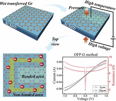
Graphene is a one-atom-thick sheet of carbon atoms arranged in a hexagonal lattice and is valued for its exceptional transparency, electrical conductivity, and mechanical flexibility. Preserving these properties during patterning is critical for device performance. Instead of removing graphene material, the OFP-G method works by selectively modifying its chemical bonds. In this process, monolayer graphene transferred onto a silicon dioxide substrate is brought into contact with a pre-etched glass substrate that defines the desired pattern.
The process is carried out under vacuum at 380 °C, where the glass enters a conductive solid-electrolyte state. When a voltage of 1,000 V is applied, mobile alkali ions migrate within the glass, creating oxygen-rich regions at the graphene interface. These regions locally convert carbon–carbon bonds into carbon–oxygen bonds only in the contact areas, producing a precise stencil-like pattern while leaving the surrounding graphene intact.
Using this approach, the researchers fabricated graphene channels as narrow as 5 micrometers. Because the method avoids photoresists and transfer polymers, the graphene surface remains clean and free of contamination. The high processing temperature also helps remove residues from earlier fabrication steps, resulting in high-quality graphene patterns. Raman spectroscopy, X-ray photoelectron spectroscopy, and molecular dynamics simulations confirmed that the patterned regions maintain structural integrity and experience reduced interfacial strain, without etching-induced defects.
Electrical measurements showed that graphene patterns with widths of 5 and 20 micrometers exhibited low resistances of 11.5 ohms and 9.4 ohms, respectively. In contrast, graphene patterned using conventional photolithography showed negligible conductivity, indicating disrupted electrical pathways caused by damage and contamination.
Because the process avoids photoresists entirely, it is particularly suitable for applications where surface cleanliness is critical, such as biosensors, neural interfaces, and nanoscale electronic devices. In the long term, this technique could help accelerate the integration of graphene into flexible and transparent electronic devices for healthcare, energy, and smart technology applications.
"Our approach offers a scalable, reproducible, and contamination-free pathway for patterning high-resolution graphene, and opens new possibilities for the integration of graphene in flexible and transparent electronics," says Prof. Jung.
Reference
Title of original paper: Direct and residue-free patterning of sub-5 µm CVD monolayer graphene with highly enhanced conductivity and pattern fidelity
Journal: Microsystems & Nanoengineering
DOI: 10.1038/s41378-025-01083-2
About Chungnam National University (CNU)
Website: https://plus.cnu.ac.kr/html/en/
Media Contact:
Gaeun Kim
+82 42-821-6239
408099@email4pr.com
![]() View original content to download multimedia:https://www.prnewswire.com/news-releases/chungnam-national-university-team-pioneers-defect-free-high-quality-graphene-electrodes-302668985.html
View original content to download multimedia:https://www.prnewswire.com/news-releases/chungnam-national-university-team-pioneers-defect-free-high-quality-graphene-electrodes-302668985.html
SOURCE Chungnam National University


